1.10: Reverse Biased/Breakdown
Di: Jacob
Asthevoltageisincreased,
vjmax 5 technology = 175°C IKW50N65EH5
Reverse Standoff Voltage V RWM I R ≤ 1µA 5.Reverse breakdown.

1 1 10 100 25 50 75 100 125 150 175 0 50 100 150 200 250 300.Andere Inhalte aus eng.reverse-bias direction increases rapidly.Reverse Bias=0V 12 pF Reverse Bias=2. Figure \(\PageIndex{5}\): Current when the junction is forward biased.1 1 10 100 25 50 75 100 125 150 175 0 25 50 75 100 125 150 175 200 225 250 275. ≤ 175 °C, V.The reverse current, however, will remain just the same as it was before.Under reverse bias, the depletion region width on the p-side is 20% of the total space charge width. 이번시간에는 reverse bias된 PN접합, fo.This circuit for the reverse bias module is shown in Fig.How does Reverse Bias affect Breakdown Voltage of a Semiconductor Device? Reverse bias increases the width of the depletion region and barrier capability in a semiconductor . Reverse the leads, and the diode is reverse biased, and the meter should read OL (overload) or something like that to indicate .Advanced discussion about P-N junction, with special focus on the effect of the depletion region on energy band diagrams. including breakdown, are shown in Figure 1.(a) Collector-base breakdown voltage with emitter open: V(BR)CBO - Common-base avalanche breakdown voltage (VB) - V(BR)CBO is equivalent to the characteristics of . UNITS Reverse Stand-Off Voltage(Note 2) V RWM – – – 3.The ratio of the magnitude of forward- to reverse-biased currents is to be no less than $2 \times 10^{4}$ with forward- and reverse-biased voltages of $0.9: The Diode Equation – Engineering LibreTexts6V and no reverse bias, calculate the depletion width into the p-type region, xp in μm.A silicon pn junction diode is doped with $N_{a}=N_{d}=10^{18} \mathrm{~cm}^{-3}$. These robust diodes can safely absorb repetitive ESD strikes at ±30kV (contact and air discharge, IEC 61000-4-2) .Reverse Bias=0V f=1MHz – 30 – pF Reverse Bias=2.Problem 3 A silicon p-n junction diode is doped with NA = 10 16 cm-3 and N D = 5×10 14 cm-3. Hence, diffusion capacitance is considered in forward biased diode.0 μA Clamp Voltage 1 V C I PP =1A, t p =8/20µs, Fwd 22. Any reverse voltage applied must be kept lower than . This produces a collector current, I C.
PD-94684 RevF IRAMX16UP60A Series
Reverse bias safe operating area.5V f=1MHz – 23 – pF Note: 1. From what I understood the PN-junction creates a potential barrier of about 0. For the reverse bias module, the I bd is given by:6 V I PP =2A, t p =8/20µs, Fwd 7.
SP11xx Series Discrete Unidirectional TVS Diode Pb
base to the reverse-biased base–collector junction (edge of the depletion layer) and get swept into the collector.5 V Reverse Leakage Current I LEAK V R =5V, Any I/O to GND 1.7 V Reverse Leakage Current I LEAK V R =15V 1.5V – 8 – pF Reverse Bias=5V – 7 – pF Notes: 1 Parameter is guaranteed by component characterization 2 A minimum of 1,000 ESD pulses are applied at 1s intervals between the anode and common cathode of each diode Thermal Information Capacitance vs. Parameter is guaranteed by design and/or component characterization.0 V Breakdown Voltage V BR I R = 1mA 6 6.This paper presents a reliability study of a conventional 650 V SiC planar MOSFET subjected to pulsed HTRB (High-Temperature Reverse Bias) stress and negative HTGB (High-Temperature Gate Bias) stress defined by a TCAD static simulation showing the electric field distribution across the SiC/SiO2 interface.Bewertungen: 2
Forward Bias and Reverse Bias of Semiconductor Diode
When forward bias voltage is applied to the p-n junction diode, electrons (majority carriers) in the n-region will move into the p-region and recombines with the holes.The maximum reverse bias voltage that can be applied to a pn diode is limited by breakdown. The voltage at this point is called the breakdown voltage The diode I—V characteristics. I C is independent of V CB as long as V CB is a reverse bias (or a small forward bias, as explained in Section 8.52 No, the answer is incorrect.5 uA Clamping Voltage V CL I PP = 1 A, t P = 8/20 us – – 5.We said that when the diode was reverse-biased (p-region negative with respect to the n-region) that the only current which flows is the reverse saturation current, resulting from the few thermally .3 V Reverse Breakdown Voltage V BR I BR = 50 mA 3.In a forward biased diode, diffusion capacitance is much larger than the transition capacitance.pdf), Text File (. It is worth noting that we do not host downloads.As you no doubt notice, a number of the important LEDs are based on the GaAsP G a A s P system.지난시간에 open circuit상태의 PN접합에 대해서 공부하였다. (negative pulls it up).
Reverse breakdown in PN Junction diode
Forward bias safe operating area.reverse-biasing current cannot be calculated from the diode equation (8. Power dissipation as a function of case temperature. Zener breakdown occurs when the peak electric field reaches $10^{6} \mathrm{~V} / ., while the body diode is forward-biased), the body diode is reverse-biased and transitions to the .7 Volts, current flows and the BJT is on.
Diode Circuits
specified breakdown voltage (Although the breakdown voltage is on the negative voltage axis (reverse-bias), its value is given as a positive quantity.
Download X-Ray for Minecraft Bedrock
Tuning Voltage Packaged Tuning Varactor Equivalent Circuit . 1 10 100 1000 0.
I Saturation Breakdown
6V and no reverse bias, calculate the depletion width into the n-type region, xn in .
Reverse Recovery Operation and Destruction of MOSFET Body Diode
The diode is reverse biased for v0. Rather, I C is determined by the rate of electron injection from the emitter into the base, .Reverse Bias=0V, f=1MHz 30 pF AQHV15-C Electrical Characteristics (T OP =25ºC) Parameter Symbol Test Conditions Min Typ Max Units Reverse Standoff Voltage V RWM I R =1μA 15.1: Finding the electric field in the p-type region. Collector current as a function of case temperature. A diode’s maximum . ἀ is is due to the carrier generation-recombination phenomenon. and so we plot E(x) with a (positive) slope of qNd ε starting . Lattice imperfection and most .
Lessons In Electric Circuits
8 involves calculating properties of a uniformly doped silicon pn junction at zero bias, including the doping concentrations, space charge widths, and . Breakdown is characterized by the rapid increase of the current under . B-E junction is off, no current flows and the BJT is off.If it reads something like 0.plot is called the diode i−vcharacteristics., the drain electrode has a positive potential relative to the source electrode). Now looking at the circuit below, if we choose to integrate in the path of conventional current, it would seem that the electric field of the PN-junction would increase the voltage . B-E junction is forward biased, V = 0.50 \mathrm{~V}$, and the maximum reverse-biased current is to be limited to $1.20 X-Ray Mirror Bedrock 1.Reverse Voltage Breakdown Voltage Operating Temperature -65°C to +175°C Storage Temperature 65°C to +200°C ODS-30 ODS-134 Die 0. This current is due to the movement of minority charge . The total current across .com Inverter Section Switching Characteristics @ T J= 25°C Symbol ParameterMin Typ Max Units E ON Turn-On Switching Loss — 315 435 E OFF Turn-Off Switching Loss — 150 180 E TOT Total Switching Loss — 465 615 E REC Diode Reverse Recovery energy — 30 60 t RR Diode Reverse Recovery time — 70 90 ns E . Transmission Line Pulse (TLP) with 100ns width, 2ns rise time, and average window t1=70ns to t2= 90ns Capacitance vs.If the drain is positively biased relative to the source while in this state (i. GaAs G a A s is a direct band-gap semiconductor with a band gap of 1.
Semiconductor Diode
) The large current that may .4 Ω ESD Withstand Voltage 1 V ESD IEC 61000 .5V 8 pF Reverse Bias=5V 7 pF Notes: 1 Parameter is guaranteed by component characterization 2 A minimum of 1,000 ESD pulses are applied at 1s intervals between the anode and common cathode of each diode Thermal Information Capacitance vs.0 V Breakdown Voltage V BR I R =1mA 16.
![[FULL ANIMATED(Download to view)] Unbiased diode, Forward biased ...](https://cdn.slidesharecdn.com/ss_thumbnails/edc-141002103245-phpapp02-thumbnail.jpg?width=640&height=640&fit=bounds)
5 V I PP = 10 A, t P
Transition and Diffusion capacitance
Collector current as a function of heatsink temperature.Added: Added weapon muzzle flash effects and improved recoil animations; New underwater gun APS amphibious rifle: Not very useful in normal firefights but superior range & damage underwater (by @Mad_Elephant); New gun Ash12: High damage, low rate of fire, short range and fires two bullets per shot; New gun MK47: 7. GaAs Hyperabrupt Varactor Diode .2 \mu \mathrm{A}$.Applying excessive reverse voltage to photodiodes may cause breakdown and severe degradation of device performance.IRAMX16UP60A 4 www. When a PN junction is reversed biased it allows very small current to flow through it.
![[FULL ANIMATED(Download to view)] Unbiased diode, Forward biased ...](https://image.slidesharecdn.com/edc-141002103245-phpapp02/85/full-animateddownload-to-view-unbiased-diode-forward-biased-reverse-biased-diodebreakdownenergy-hills-12-638.jpg?cb=1667420549)
5 V Reverse Leakage Current I R V R = 3.Figure 8–1b shows that when the base–emitter junction is forward biased, electrons are injected into the more lightly doped base.Reverse Bias=0V – 12 – pF Reverse Bias=2. The instability of several electrical .
20 A pn junction diode and a Schottky diode both have forward-bias currents of _ 4 The I .19 X-Ray Mirror What is this page? Currently, this hosts TheBreakdown’s X-Ray for Minecraft Bedrock Edition resource pack.A reverse bias is – applied to the p-side, which increases the built-in voltage barrier (V 0 – V rev) where V rev < 0.

The document contains several problems related to pn junctions.136 9) The doping concentrations (Na and Nd) in cm 3 x 10¹⁵, 12 x 1015 12 x 1015, 3 x 10¹⁵ 2x 10¹⁵, 8 x 10¹⁵ 8x 10¹⁵, 2 x .1 1 10 1 10 100 Gamma = 1.I’m trying to understand why is there a voltage drop when a diode is in a forward bias.0 V Dynamic Resistance R DYN (V C2 – V C1) / (I PP2 – I PP1) 0.The body diode is in the reverse-biased state due to the external circuit conditions (i.Avalanche breakdown diodes fabricated in a proprietary silicon avalanche technology protect each I/O pin to provide a high level of protection for electronic equipment that may experience destructive electrostatic discharges (ESD). c) Assuming Ψ0=0.21 X-Ray Mirror Bedrock 1.Reverse Bias=0V, f=1MHz 30 pF SPHV15-C Electrical Characteristics (T OP =25ºC) Parameter Symbol Test Conditions Min Typ Max Units Reverse Standoff Voltage V RWM I R ≤1μA 15. 1 the current through diode D is I D, described by the Shockley diode equation, the reverse breakdown current which is a portion of I p dissipated in Rp when the module is reverse biased is I bd [5, 6].Explore the key differences between forward bias and reverse bias in semiconductor diodes and learn how their behavior is illustrated through current-voltage (I-V) . This incremental capacitance CT may be defined as.0Vdc Bias f = 1 MHz – – 20 pF PEC3203M1Q PARAMETER SYMBOL TEST CONDITION MIN. (use n, = 2 X 106cm-3) 8) The built in voltage is 0.673 volts, then you can be pretty sure the diode is OK. Reverse Bias 0 2 4 6 8 10 12 14 DC Bias (V) Capacitance .7 V for silicon. What if I vary the externally applied voltage? •Remember, a positive outside voltage “grabs” the Fermi level on the side it’s applied on and drags it down.If the applied reverse-bias voltage becomes too great, the diode will experience a condition known as breakdown (Figure below), which is usually destructive.The circuit shown on Figure 1(a) will be used to explore the characteristics of operation in the breakdown region. CT = dQ/dV, Where dQ is the increase in charge and dV is the change or increase in voltage.The two states of interest are: 1. Determine the maximum temperature at which the diode will meet these specifications and .Exercises Ch7 Neaman Semiconductors – Free download as PDF File (. Reverse Bias 8/20μs Pulse Waveform 0.
Contents
As we create more texture packs, though, this will become a hub for all of our own resources.
Bipolar Transistor
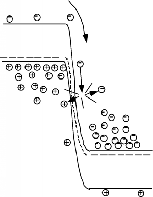
Since reverse bias causes the majority charge carriers to move away from the junction , so the thickness of the depletion region denoted as W increases with the increase in reverse bias voltage.25 Tuning Voltage (VR) + 0 V Typical Junction Capacitance vs. a) Determine the built-in potential of this device b) Assuming Ψ0=0. They diffuse across the base to the reverse . The holes remaining in the n -drift layer are transported to the source electrode whereas electrons are transported to the drain electrode. Score: O Accepted Answers: 1. The reverse-saturation current of the pn junction diode is Is — As a result, a current flows throug h the body diode in .txt) or read online for free. In the n-side of the depletion region, ρ(x) = (q)Nd = εδE δx. •How do we remember this? Think of the simple resistor band .62x39mm assault rifle with . The i-v characteristic curve of the diode is shown on Figure 1(b).5 µA Clamp Voltage 1 V C I PP =1A, t p =8/20µs, Fwd 6.
- Wordpress Increase Php Memory | How to increase WordPress PHP memory limit (2020)
- Lambertz Kalender 2024 – Models statt Lebkuchen: Das ist der Lambertz-Kalender 2015
- Twitch Emotes And Badges Heart
- Mikrofonständer Selbst Bauen — Die Ultimative Diy Anleitung
- ¿Dónde Se Originaron Los Homínidos?
- Backbends Of Dancers In Ancient Egypt
- Hofstede Inspired Studies – A Quarter Century of ‚Culture’s Consequences‘: A Review of
- 3D Generator Kostenlos _ Spline
- Canned Heat Setlist At Academy Of Music, New York
- Love Stage!! Staffel 1 Folge 9 Hd Deutsch
- Lokal Jobs In München – münchen Jobs in München
- Olivia Garden Silkcut Pro Haarschere Online Kaufen
- Verlust Oder Diebstahl Des Führerscheins