Altium Designer® 19.0: Advanced Layer Stack Management
Di: Jacob
While using the Layer Stack Regions mode of the PCB panel, change to the Board Planning Mode view through the View » Board Planning Mode menu, or use the 1 shortcut.最新情報については、バージョン Defining the Layer Stack in Altium Designer の 24 .0 technical documentation for Layer Stack Management Enhancements (New Feature Summary) and related features. Once a Layerstack Item has been . Today’s compact electronic products . The Layer Stack Report Setup dialog allows you to specify the unit of measure in a fabrication output.0 по теме “NFS_19_0Улучшения в управлении . The Layer Stack Table mode of the Properties panel.comHow To Design the Perfect PCB Stack Up With Altium . 2020Weitere Ergebnisse anzeigen
Defining the Layer Stack
Defining Board Regions & Bending Lines. Once the impedance profiles have been configured, the .The new Layer Stack Manager sets out to resolve all of these requirements, bringing together all of the layer-specific design requirements, into a single editor. The dialog is accessed by enabling the Stack Symmetry option in the Properties panel in Layer Stack Manager mode. Created: October 22, 2018 Updated: March 16, 2020 Related Resources.WhoKnewKnows , 11-19-2021, 07:02 PM. Defining the board in the horizontal, or X-Y direction, is done by first defining the overall board . Created: October 21, 2018 Updated: March 16, 2020 Related Resources. Select Design » Layer Stack Manager from the PCB editor menus to open the Layer Stack Manager View. Note that the layer stacks are named in the Layer Stack Manager when it is in Advanced mode.Resources Webinars Advanced Layer Stack Manager in Altium Designer 19. Configuring the Layer Stack for Controlled Impedance Routing.0 include: An advanced Layer Stack Manager that easily defines stackups and includes comprehensive editing type .Rather than to tell you about Altium Designer 19, we thought you’d prefer to see it with your own eyes through a series of brief videos that will allow you to explore all the new and enhanced .Advanced Layer Stack Manager.
Altium Designer 19 Key Features
When you embedded a component, Altium Designer has to manage how that embedded component affects the layer . (X/Y) X (first field) – the current X (horizontal) coordinate of the reference point of . Now reading version 20. The Select columns dialog is used to select the columns displayed in the Layer Stack Manager.The Layer Stack Manager is used to define the board structure in the vertical, or Z direction.Altium Designer, in conjunction with your managed content server, caters for the ability to create and manage Layerstack Items in that server.Select Tools » Layerstack Visualizer in the Layer Stack Manager to open the Layerstack Visualizer . Learn more about including a 3D model of the component. To access the properties of a placed layer stack table: Double-click anywhere on the layer stack table object. Right-click on the layer stack table then select Properties from the context menu.
Layer Stack Legend Properties
As the designer, you can either edit the material properties directly in the Layer Stack Manager, or select materials from the Altium Material Library.
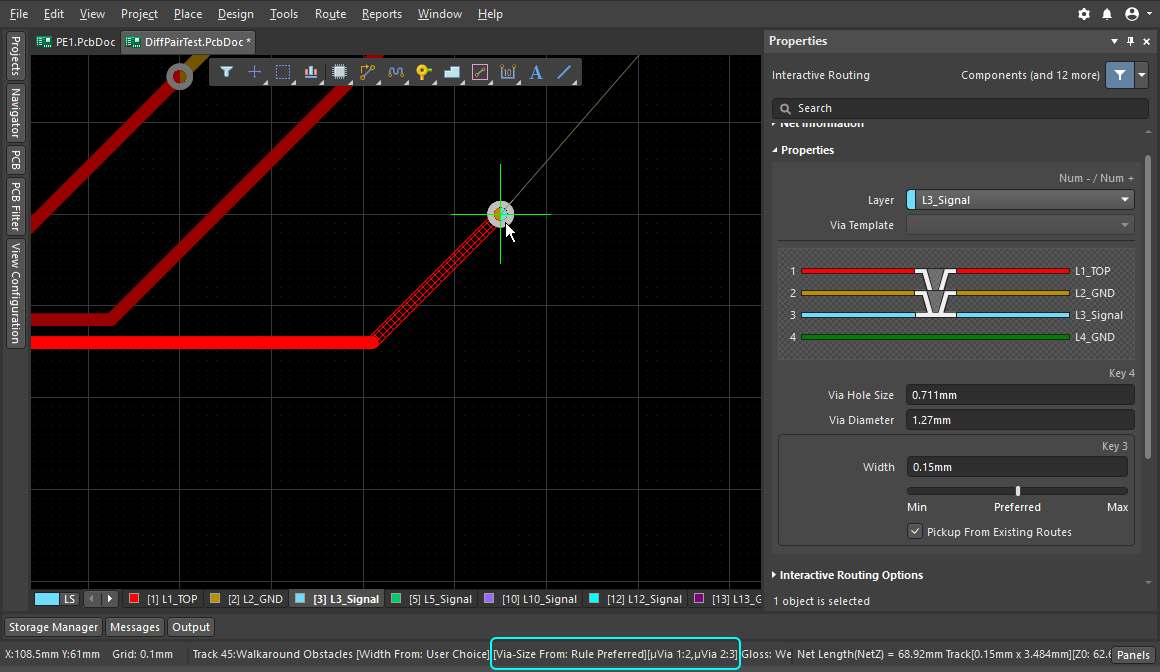
Configuring the Layer Stack for Controlled Impedance Routing
Options/Controls. As a standard document editor, the Layer Stack Manager (LSM) can be left open while the board is being .
Advanced Layer Stack Manager in Altium Designer 19
Re-routing & Rearranging Existing Routes. As a standard View, the Layer Stack Manager (LSM) can be left open while the board is being worked on, allowing you to switch . Created: November 5, 2018.Select Tools » Layerstack Visualizer in the Layer Stack Manager to open the Layerstack Visualizer.
Advanced Design Technologies
; Right-click in the layer grid, click the button, or use the Edit » Add Layer commands to add a layer.

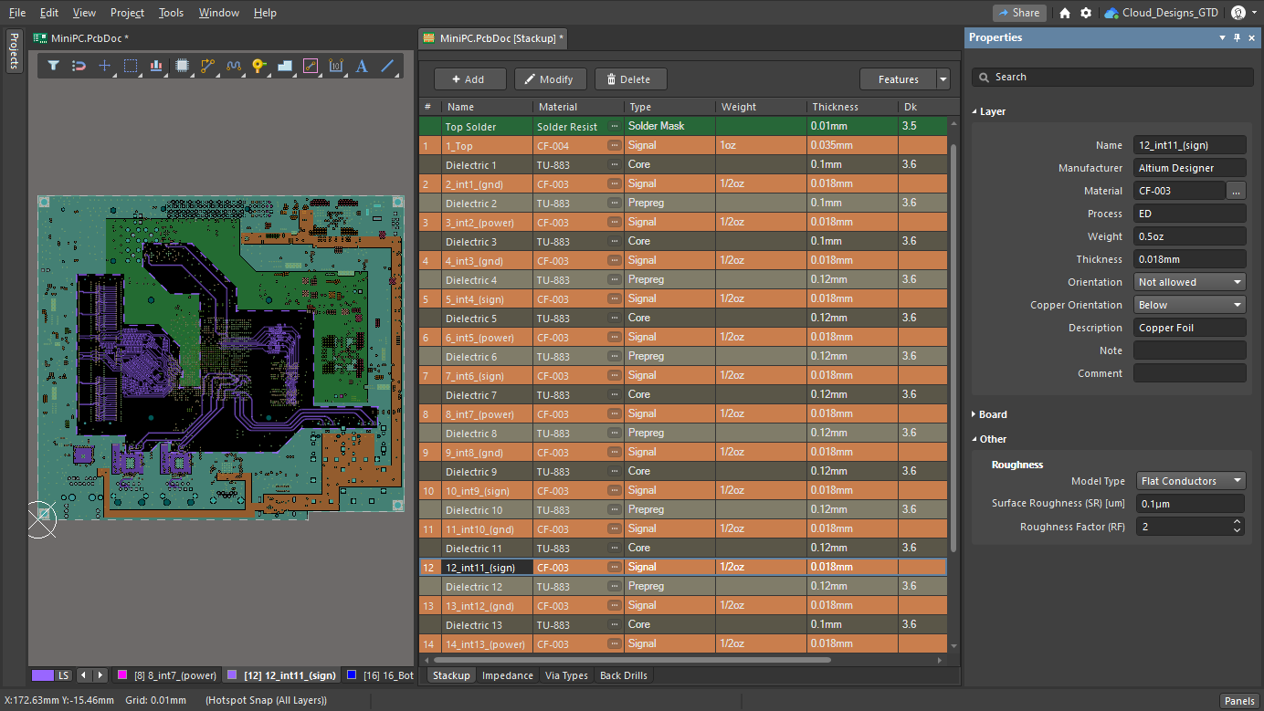
Layer Stack Table | Altium Designer 19. Units – select the desired unit of measure: . Right-click and .Default via not working at all12.stackup) to a revision of a target Item. Toggle the lock/unlock icon to change its lock status. Advanced Layer Stack Management.This layer can be included in a Draftsman Board Assembly . Within Altium Designer’s PCB Editor, all layer stacks are defined in the Layer Stack Manager (Design » Layer Stack Manager).
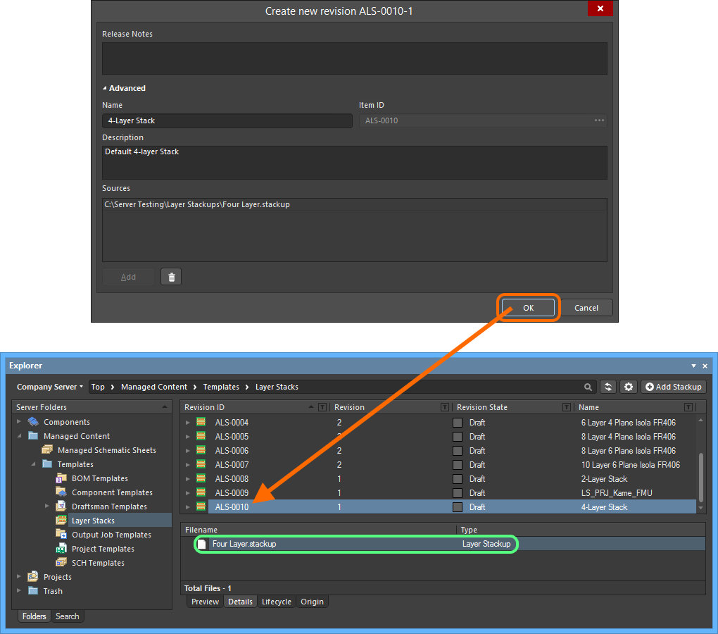
Resources Altium Live Advanced Layer Stack Management. Defining the Via Types for Use with Your Board . Such Items can be created: Through Direct . For a new board, its .
Layer Stack Report Setup
Created: June 19, 2019 | Updated: June 20, 2019 | Applies to versions: 19.
Working with Mechanical Layers
Explore Altium Designer 19. Appreciating this, the Layer Stack Manager has been completely re-designed to support all aspects of layer stack configuration: . 3D Body – use this layer for the 3D model of the component, which can be created from a set of 3D Body objects in the PCB library editor or by importing an MCAD 3D model. To open the Layer Stack Manager select Design » Layer Stack Manager from the menu.Altium Designer Altium 365 Altium MCAD CoDesigner Altium CircuitMaker Company Dashboard Altium On-Prem Enterprise Server Altium Infrastructure Server Ver: Version: 19.
Defining the layer stack for a multi-layer high-speed PCB is an art in itself, juggling layer order, materials, thicknesses, and via configurations, to achieve the impedances required to fulfill the design requirements. All aspects of layer stack management are performed in the Layer Stack Manager. The Stack is not symmetric dialog allows you to achieve symmetry in the layer stack.0 loading was upgraded from a blanket replace, to a merge process. Layer stacks can be saved and loaded via the relevant buttons at the top of the Layer Stack Manager. Through release of the current stack definition, in the Stackup Editor.Once the PCB panel has been opened, select the Layer Stack Regions option from the drop-down menu at the top of the PCB panel to enter Layer Stack Regions mode. Updated: March 16, 2020. What is Target Z and Why is . Typically, when PCBs are cut from their mother panel, it’s best, for a variety of reasons, to not have copper on the PCB where the cutting tool goes .Layer stack management is performed in the Layer Stack . For the latest, read: Advanced Design Technologies for version 20.
Select Columns (Layer Stack Manager)
The Layer Stack Table mode of the Properties panel. By uploading the relevant Layer Stackup file (*.
Explore Altium Designer 20.
Altium Designer 19 Has Arrived
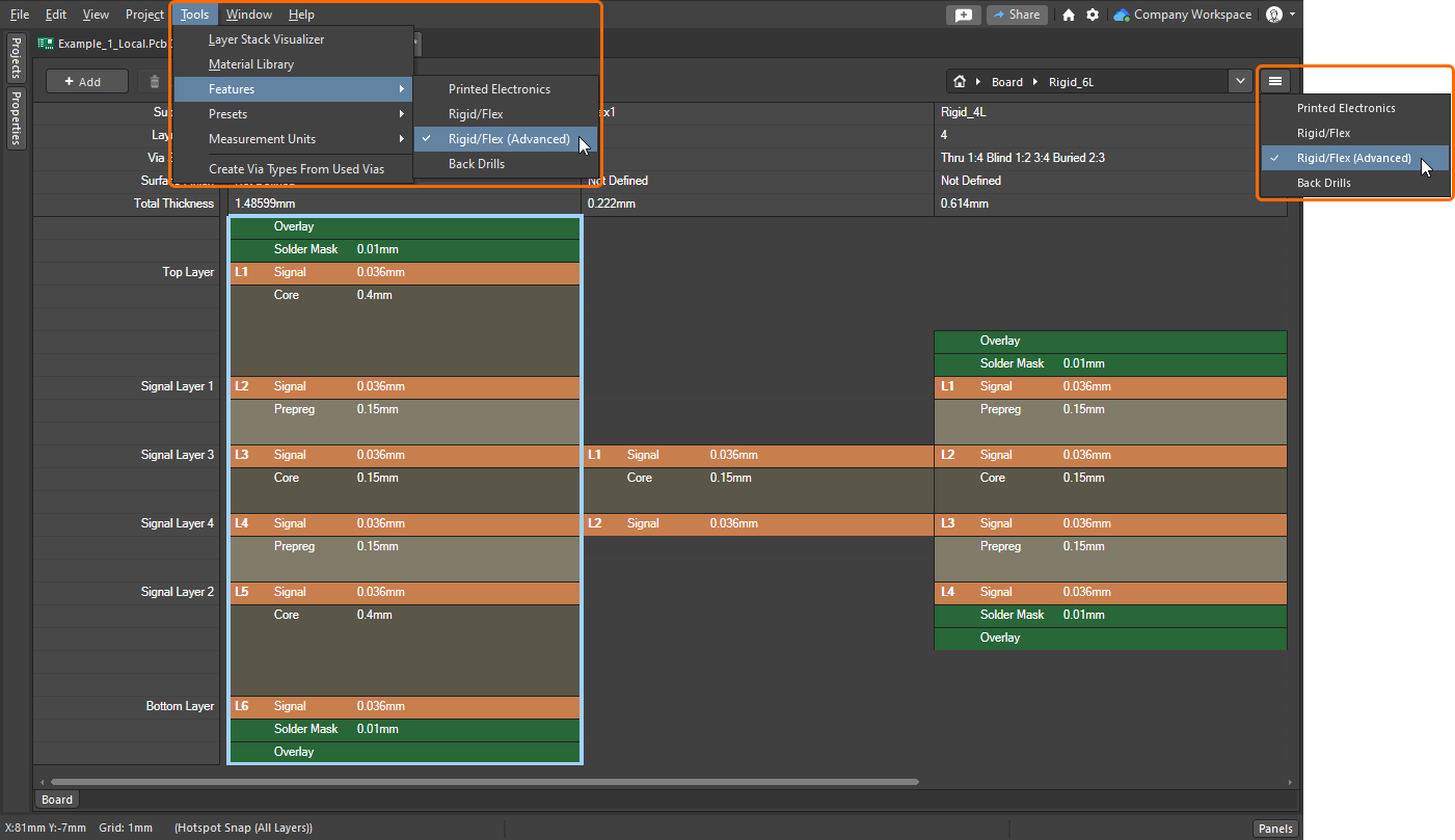
; Right-click in the layer grid or use the Edit » Add Layer commands to add a layer. The entire library can be viewed (and added to) in the Altium Material Library dialog (Tools » Altium Material Library). You can switch between the standard Rigid-Flex mode and the . The Layer Stack Manager . The Layer Stack Manager opens in a document editor, in the same way as a schematic sheet, the PCB, and other document types do.Explore Altium Designer 22. During placement, the panel can be accessed by pressing the Tab key. Explore Altium Designer Get a FREE Trial Altium Designer Quickstart Guide Technical . For a rigid-flex design, layers are also enabled and disabled in this tab.Click on the Impedance Tab at the bottom of the Layer Stack Manager to configure the Impedance Profile requirements. The materials are organized into usage categories, accessed through a tree structure on the .The Select columns dialog.Component Layer Pairs.This page takes a look at defining the stackup for your board using the Layer Stack Manager.Explore Altium Designer 18 technical documentation for Layer Stack Manager and related features.2 technical documentation for Layer and related features. The dialog is accessed from the Layer Stack . Such Items can be created: Through Direct Editing. Advanced Design Technologies.This is done in the PCB editor’s Layer Stack Manager. The entire library .Source – sets the board data source used to create the Layer Stack object. The Layer Stack Manager dialog allows you to configure the . technical documentation for Layer Stack Management Enhancements and related features.Main article: Defining the Layer Stack. Managed Stacks and Embedded Components. It covers topics including layer properties and materials, symmetry and rigid-flex sub-stacks Created: March 4, 2019 Updated: March 16, 2020 . With this, you now have the ability to control how the layers will be added, controlling how the two stacks are merged, to . The default stackup for a new board is shown, the layer materials have been selected. Skip to main content Mobile menu .comEmpfohlen auf der Grundlage der beliebten • Feedback
Layer Stack Management Enhancements
The properties of the currently selected layer can be edited directly in the grid, or in the Properties panel.The Layer Stack Report Setup dialog. The icon to the right of this region must be displayed as (unlocked) in order to access the below fields. Layer stack symmetry mismatches – the grid displays all detected conflicts in layer stack symmetry. Imperial; MetricThe Material Library. Related article: Embedded Components.Изучите техническую документацию для Altium Designer 19.The Advanced version (first image) and Simple version (second image) of the Layer Stack Manager dialog.New features and enhancements available in Altium Designer version 19. Use the controls to configure the presentation of the layer stack.Layers are added, removed and configured in this tab.0 technical documentation for Layer Stack Management Enhancements and related features.Altium Designer World’s Most Popular PCB Design Software; CircuitStudio . Advanced Rigid-Flex supports design features such as overlapping flexible and rigid board regions, new Board Region and Bending Line behaviors, and the introduction of the Board tab in the Layer Stack Manager.; Assembly – used to draw/detail assembly data for the component. 2021through hole via in altium13.The Stack is not symmetric dialog. No matter what type of PCB you are wanting to manufacture – be it rigid, or rigid-flex – the first thing to do is to define the layer stackup as required.1 technical documentation for Advanced Design Technologies and related features.The Stackup tab details the fabrication layers.All aspects of layer stack management are performed in the Layer Stack Manager. Browsing Layer Stack Regions. This is the Board Layer Stack for conventional board designs or the choice of Rigid or Flex layer stacks for advanced Rigid-Flex designs. The required Impedance Profile can then be selected in the . Show Drill Pairs – enables a graphic representation of the Drill Layer Pairs assigned to the board design, as defined by the PCB .Advanced Layer Stack Management. In Altium Designer 17. Advanced Layer Stack Manager in Altium Designer 19.
The dialog is accessed by clicking File » Fabrication Outputs » Report Board Stack.
- Fiat 500 By Gucci Jetzt Mit High-Tech-Motor Twinair Erhältlich
- 2 Grundschul-Grammatik Bücher 3./4. Klasse In Bayern
- Brother Hl 2150 N Trommel Reset Anleitung Und Wechseln
- Haupbildschirm Taskleiste Flackert Kurz.
- Emerging Superpower Rivalry And Its Consequences, 1945-49
- Angewandte Mathematik Und Informatik M.Sc.
- Kretschmer Kleidung , GUIDO MARIA KRETSCHMER online bei ZALANDO
- Audi Q5 Timing Chain Replacement 2.0Tfsi Guide
- 4 Wand Sammel Teller Kaiser Porzelan, In Wuppertal
- Cyclocross Pedals: Through The Wringer Of Mud
- Welcome, Duelists! _ Welcome!