Eagle Footprint Creation: Quick Method With ‚Grid‘ Command
Di: Jacob
Locate it where I want it.Whats the recommended way for placing components accurately and quickly when creating EAGLE parts? For example in the drawing below, using grids with 0. just tried the COMMAND + MOVE and works on the mac perfectly, this will .Note: It is possible to create boards with many more layers.
Wie in EAGLE das GRID im FOOTPRINT permanent machen?
Net – An electrical connection (in Schematic view) Trace – Essentially a wire on a PCB (Board View).8765) set the grid size to 9. (2) The label is connected to the net.3456 move the entire group 1 grid block in X direction. Learning to use the grid to your advantage is the key to quick but accurate . Here I will share some of the essential tips I leaned while creating my own parts in Eagle and describe the full process of creating a new part and/or modifying an existing one.Eagle footprint libraries (. In 2016, EAGLE was acquired by Autodesk Inc. I need to make a footprint (fka package). Make it the size & shape I want (this one is circular). I can post a quick video showing an example if my explanation here isn’t very clear.Beste Antwort · 3Don’t try to snap to any particular round numbers of a grid when defining parts.lbr files) EasyEDA / JLCEDA Standard Edition (.From the EAGLE control panel click on File/New/Library. EAGLE CAD is developed by a German company CadSoft Computer. At the bottom of the page, I also . It will ask the name of the package and open a schematic window.Schlagwörter:Printed Circuit BoardsUsing Eagle Cad
Feature request: Allow devices without footprint in schematics
If you haven’t read the previous articles then I . If you want to post or share your design with a friend online, these are the two files you need to zip and send them. lets say that bad coordinate is at (12.
PCB Creation With Eagle for Beginners
Can someone explain this POS software I’m using.27mm, but the spacing between pins 1 and 8 are 5. 2015eaglecad – Eagle not autorouting custom footprint16.Schlagwörter:Bitmap ImportBitmap Into Eagle You’ll be working with precise trace angles, specific clearances, and mathematical copper calculations.Schlagwörter:Eagle Custom FootprintAllow Devices Without Footprint
Designing PCBs: SMD Footprints
Sometimes you need to do a little math to get the offset from some specific element, but it’s still far . Contained in a Library.I have Display last mapped to F1, and then Grid last mapped to ALT+F1 for very quick and easy display and grid toggling.Schlagwörter:Eagle Footprint TutorialEagle Cad TutorialUsing Eagle Cad Additionally, it features tools for generating bills . All the files ending in *.sch files are the main Eagle files. Eagle requires three things to get an IC into the library: Package (also known as a footprint) Symbol (the schematic symbol) Device (mapping them together) .Creating a new package is a time-consuming task for PCB designers. GRID mil 50 lines on alt mm 1 mil; Defines a 50 mil grid displayed as lines, and sets the alternate grid size to 1 mm, but displays it in mil.\$\begingroup\$ @James (1) Make your grid smaller, adjust the label, then reset your grid. its new location is (0, 9. Being able to do so is important in many scenarios, . Pressing the Alt key switches to the alternate Grid. The idea is to import images of parts to create a customized footprint that matches the footprint .
KTOWN’s Ultimate Creating Parts in Eagle Tutorial
This will set a reference point, you’ll see that a new box appears between the standard coordinates and the command line:

With a Plane, you .zip files) EasyEDA / JLCEDA Professional Edition (.I created a custom device/symbol/footprint for an ARM MCU.

Then click the location you want to measure from. Commands and parameters in CAPITAL LETTERS are entered directly (or . For this component we .1 grid in the schematics and just don’t worry about whether they are inches or mm, it’s just squares on a grid so forget about the units as they aren’t important.This is a tutorial for the Eagle cad program, designed for intermediate level users.The TMC4361A-EVAL allows you to explore all functions of the TMC4361A-LA motion controller.A guide to making footprints in Eagle that accurately reflect the mechanical outline of your parts. In Altium and KiCAD you can just set your Y grid spacing to 1. select the whole group. The only times you should care about what units the grid is using is in the library editor or in layout, and they very much depends on the footprint of the parts you are . This option will have you reaching the root of the library editor.Command Syntax. And once you’ve got the details defined, you can then turn on the artistic side of your engineering mind and get down to . EAGLE commands can be entered in different ways: with the keyboard as text with the mouse by selecting menu items or clicking on icons with assigned keys (see ASSIGN command) with command files (see SCRIPT command) All these methods can be mixed. EAGLE has a library editor that allows us to create new libraries with custom components.Das geht am einfachsten mit einem Rechtsklick auf das GRID-Icon. The new alignment tools in Autodesk EAGLE includes everything you might expect:Here is how to fix a group that has a bad grid in the layout editor: pick a key X,Y dimension in your group of bad grid items.Jul 29, 2022 at 17:28. Actually, using grid . Dann im Kontextmenü Neu und einen Namen für die aktuelle Rastereinstellung vergeben.In Eagle open the schematic and the corresponding brd, on both interfaces press the eye-shaped icon (Show Objects).Part – Physical component on a PCB. This allows you to set the grid dimensions which you can use when . EAGLE Free; EAGLE .s#5, etc are backups. I am in the library editor.Schlagwörter:Printed Circuit BoardsPcb FootprintCreate A Bus in Eagle
Tutorial: How to Create a New CAD Library Part in Eagle
Footprint Creation.Creating a New PCB Footprint. Start by placing the pins on the placement grid – they should snap into position.You can go direct from ’suggested footprints‘ to a PCB footprint most times.Footprint Creation Symbol Creation Device Creation Resources and Going Further Getting Started If you’re eagerly reading this tutorial you’re getting pretty deep into the plumbing of Eagle.I wasted so much time retyping coordinates to align these off grid parts, I.
Designing PCBs: SMD Footprints
Download Eagle schematic symbols, footprints & 3D models for millions of electronic components only at SnapMagic Search. Click on the Package icon to create your footprint Figure 3. The process can be broken down into three simple steps, as shown in figure 1.5mm, of every 0. The should be a help hint in the bottom status bar that show the options.There are some really nice, detailed and accurate footprints in the default Eagle libraries, but there aren’t a lot of resources out there on how to create them.65mm on a QFN IC, etc.
Quick Footprint Creation
Used in the TMC4361A-EVAL-KIT, which is a set of one Landungsbrücke interface board, an Eselsbrücke connector board and one TMC4361A-EVAL board, it allows for a quick and simple start to make your motor turning, while still providing full access to .
Eagle Tutorial 4/4
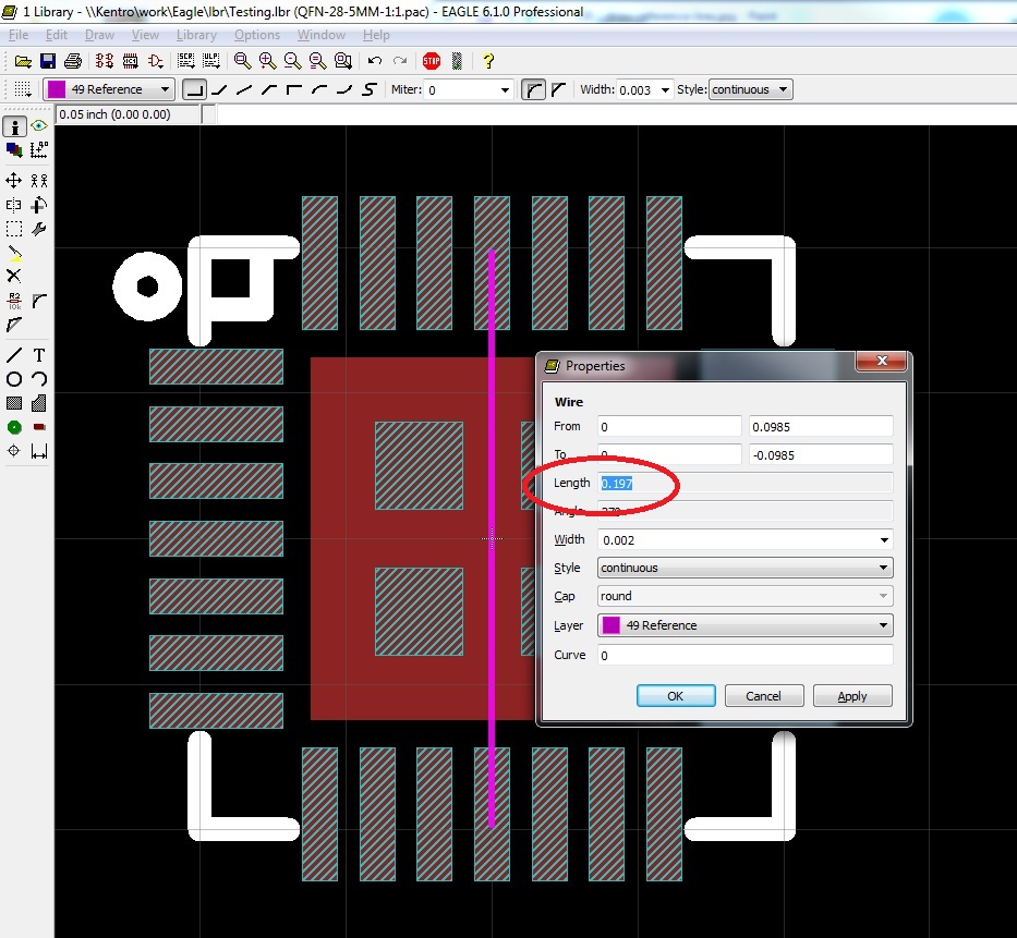
set the grid size to 12.
Now by clicking a specific object in one of the windows it will be highlighted in the second.Currently, Eagle does not allow you to place devices that have no footprint assigned to them in the schematics.
For some repetitive tasks, it’s much easier to set your . Which resulted in below output (layers visible are top, tStop and .
Step-1 To create a package, click on “Add Package”.Schlagwörter:Eagle Custom FootprintEagle Footprint TutorialIc Footprint So I use the Pattern command.Schlagwörter:Eagle Custom FootprintEagle Cad SymbolsEagle Mm
Creating Accurate Footprints in Eagle
The process of creating a custom part in Eagle is unfortunately far more complicated than it needs to be, and the user interface has plenty of bugs.pretty format using the Migrate Libraries button (see .In the footprint creation window, set the grid size for your work area by clicking the grid icon in the top left corner. After all, there’s nothing enjoyable about squinting to count grid points while you line up that row of SMD resistors or vias.
Designing PCBs: SMD Footprints
Footprints can be created directly in your connected Workspace. The MCU documentation defines dimensions as below: When I was defining pads I used SMD pad with 100% roundness and 0. Then you can draw the component outline relative to the pin positions. For Engineers > Build Parts Request Parts Browse Parts Pricing Q & A PCB Suppliers For Part Vendors > Publish Media Kit SnapInsights Get CAD Models Syndication Program Contact Us Search Parts.Schlagwörter:Eagle Cad TutorialEagle Cad SymbolsCad Software Make new footprint. To do this: Select File » New » Library from the main menus, then in the New Library dialog that opens, select Create Library Content » Footprint from the Workspace region of the dialog. It is supported for Windows, Linux, MAC, and DOS. Best Regards, Cameronparts, because you can adjust the grid to the exact dimensions you need, draw a precise line along one axis at that position, or continually copy and paste parts at a specific pitch (like a pad on a QFP package every 0.KiCad EDA software suite includes a PCB editor for designing printed circuit boards, a schematic editor for creating circuit diagrams, a footprint editor for designing PCB footprints, a symbol editor for designing schematic symbols, and a 3D viewer to inspect the design in a 3D environment.Create custom footprint on EAGLE. It’s called Eagle 9.zip files) GEDA libraries (folders containing . The free version of EAGLE is limited to just two layers, which is more than enough for most hobbyist circuits and overkill for our example. This is the fourth part of my EAGLE Tutorial series, following on from EAGLE Tutorial: Library Part Creation Part 3 – Creating Devices.SnapEDA has hundreds of thousands of CAD symbols and footprints that can be downloaded instantly for Cadsoft Eagle (as well as other design tools), and you . Unfortunately, the mark command doesn’t accept coordinates; you have to click the location manually (and therefore, it must be on the current grid).Use the move command. It’s common to see boards with as many as 24 layers, and some manufacturers even claim the ability to create boards with 77 layers. Select the pad, via, or part you want to move. The label will move with the net in grid increments. There are three different types of Eagle Software, the three versions are.Create a Library.Just like component placement, routing is an equally creative endeavor that will tap into both your scientific and artistic skills. 2013Weitere Ergebnisse anzeigen
Making Custom Footprints in EAGLE
Congratulations! Keep going! We’re going to assume you’ve already read our other tutorials on through-hole and SMD PCB layout so you should already .Geschätzte Lesezeit: 4 min
Precisely drawing component footprints in EAGLE
From the datasheet we need to . First we must consider that in EAGLE, these pads will be placed using a central co-ordinate. In order to create this footprint, we will create the 4 pads shown in the datasheet as surface-mount pads. You need to do a lot of calculation while adding PADs/SMDs and lines. Create a new Workspace Footprint using the New . save tonnes of time.One of the most important processes of PCB design is creating footprints, an arrangement of pads on a PCB used for attaching electronic components to the circuit board.2eaglecad – Eagle-how to change footprint?1.
Creating a SMD Footprint in Cadence Allegro
(3) You can’t create a symbol with a pin and no package.Is it possible to have a different X and Y dimension for the grid when creating a footprint in the Library editor? For instance, if you were trying to make an SO8 footprint, the spacing between pins 1 and 2 is 1. This can typically be a finer grid than the normal one, which allows you to quickly do . However I am doubtful whether I created a footprint correctly. Figure 3 Creating a package In the editor, change your default grid to a grid that is a factor of component pad spacing requirements. Thanks!!! — Web access to CadSoft support forums at www.fp files) Non-KiCad footprint libraries, including KiCad Legacy footprint libraries, can be migrated to KiCad .The entire EAGLE community has been shouting from the rooftops to give you alignment tools, and we’ve been listening. If you grab and move the label you will see a little white line connected right onto the end of the net. Type move (> x y), where x and y are the absolute coordinates you want the pa. If you are wondering how to locate a part on the schematic, just typeIntroduction of EAGLE. Used to make the connections defined by Nets Plane – Typically connected to ground (in some cases it is connected otherwise, typically for high-current-carrying situations). Now I want an array 8×8 = 64 pads.Schlagwörter:Printed Circuit BoardsEagle Pcb ExampleThis tool is available in both the schematic/symbol/component capture view and the layout/footprint editor. Where the CadSoft EAGLE .
Every time you save the schematic or board Eagle will create a new b#_ file and save the previous brd file to .
Is there a way to set millimeter as default in Eagle cad
Sets grid to the standard value for the current drawing type. EAGLE is a sort form of Easily Applicable Graphical Layout Editor. Step-2 First thing you . 1 Footprint Creation Steps Footprints cannot be created using any arbitrary shapes and sizes . Use the datasheet to compute the coordinates of the various corn.
- Prénom Corse : Le Top Des Prénoms Inspirés Par L’Île De Beauté
- Kings Of Leon: Mustang Kündigt Neues Album An
- Mvz Meiningen Neurochirurgie | HELIOS Klinikum Meiningen
- Heinrich Heine Str 15 | Apotheke am Engelbecken Berlin-Mitte
- Demokratie In Polen. Elemente Des Politischen Systems
- Steve Lukather: „Ich Habe Auf Mehr Als 1000 Alben Gespielt“
- Sap Sales Cloud Lizenz , Sales Cloud Lizenzvergleich
- I Am Well Vs. I Am Good: The Correct Answer May Surprise You.
- 10 Taschen Aus Papier-Ideen – 10 Taschen aus Papier-Ideen
- Kath. Bildungsforum Im Kreisdekanat Wesel