Esd Precautions For Die/Wafer Handling And Assembly
Di: Jacob
4 Product Handling & ESD Precautions Static Control Work Station It is recommended that all areas where ESDS devices and assemblies are handled outside their Manufacture machines for the semiconductor industry, wafer handling tools, vacuum wands, tweezers, die handling, lense handling, electronic component handling.

Proper handling procedures for ESDS. Standard ESD precautions and safe work environments are as defined in MIL-HDBK-263.
GaAs MMIC Handling and Die Attach Recommendations
com Document No.Document information AN10706 Handling bare die Rev.
AN10706 Handling bare die
*D 3 Q: What are Cypress’ storage recommendations? A: .
Die singulation, also known as wafer dicing, is reviewed in terms of the brief history, critical challenges, characterization of singulation quality, different singulation technologies and .C E EGCD G Features • Low VCE(sat) = 2 V (typ. At circuit level, human body model (ANSI/ESDA/JEDEC JS-001) describes ESD waveform and test method approximating the discharge from the fingertip . In this webinar, industry experts in Hi-Rel power electronics design, packaging, testing, and qualification of Hybrid and Space-Grade PCB DC-DC power supplies, will provide the latest options and best practices in realizing the optimal power supplies for .June, 2019 Test Technology HIR version 1.3 Die Size and Tolerance of Bare Die Products The die size that described in our product development specifications is the width betweencom 1 AN-1060 International Rectifier • 233 Kansas Street, El Segundo, CA 90245 ! USA BARE DIE: HANDLING AND STORAGE By Richard Clark Introduction .
ESD in Electronics Manufacturing: What PCB Engineers Should Know
The strap prevents .1 When protection is off: transparency.To avoid ESD when handling or storing IT equipment, you should wear clean and dry clothes made of natural fibers, such as cotton or wool.October 2017 DocID027350 Rev 2 1/10 This is information on a product in full production. Handling Precautions and Storage Silicon dies must always be handled with .ACSN-04: Reconstructed Wafer Packaging Introduction PDF: 09005aef834eb5b4/Source: 09005aef834eb5af Aptina Imaging reserves the right to change products or specifications without notice.
Towards efficient ESD protection strategies for advanced 3D
Dateigröße: 1MB
Long Term Storage of Wafer and Die Semiconductor IC Products
6 Application Note Silicon Capacitor – Recommendations to handle bare dies 1.SZZA027A Electrostatic Discharge (ESD) Protective Semiconductor Packing Materials and Configurations 5 Figure 1.Download scientific diagram | Alignment, bond and assembly comparison for die to die, die to wafer and wafer to wafer assembly.com for sales contact information.Bare Die Products Handling and Operating Manual(Rev. Product must be handled only .Industry Council on ESD Target Levels Aspects of System Level ESD 4 Introduction! Component Level HBM/MM (according to ESDA, JEDEC or similar standards) addresses . 02 — 10 June 2011 Application note Info Content Keywords bare die, handling, ESD, clean room, mechanical . Company Address: 10961 Bloomfield St.01 Mar 2024: This standard applies to devices susceptible to damage by electrostatic discharge greater than 100 volts human body model (HBM) and 200 volts charged device model (CDM). Phone: (562) 594-4631QORVO WHITE PAPER: GaAs and GaN Assembly and Handling Procedures Page | 2 GaAs and GaN Die Assembly and Handling Procedures Component Placement Note . In the electronics industry, ESD can be extremely damaging to sensitive components such as integrated circuits, semiconductors, and printed circuit boards. Wrist straps can control static charges on the personnel handling ESDS .Additional information 4 of 19 Revision 3.P a g e | 3 Aviation Suppliers Association Best Practice Handling of ESD Sensitive Parts for Distributors Copyright © 2020 Rev 2 Purpose and AudienceProduct must be handled only at ESD safe workstations.org/hir) Chapter 17, Page 35 Heterogeneous Integration Roadmap Section 7: Wafer Probe and Device Handling
PCB Design and Assembly for Flip-Chip and Die Size CSP
This article discusses some guidelines on handling and storage of Allegro devices regarding its functionality and shelf life.10 2023-03-13 Recommendations for board assembly of Infineon optical sensor packages with ball grid array
Fundamentals of ESD Protection at System Level
To avoid over-design of ESD protection, .ACSN-06: ESD Precautions for Handling & Assembly Introduction PDF: 09005aef835da9f7/Source: 09005aef835da9fa Aptina Imaging reserves the right to change products or specifications without notice.2 Protection against ESD.com STG25M120F3D7 1200 V, 25 A trench gate field-stop M series
Sustainment
com IR WORLD HEADQUARTERS: 233 Kansas St. It also includes safety measures against ESD (electrostatic discharge), moisture, and contaminants that are essential for these electronic devices. 02 — 10 June 2011 Application note Info Content Keywords bare die, handling, ESD, clean room, mechanical damages, delivery forms, transport conditions, store conditions) 6 Wafer IRFC3810B HEXFET Power MOSFET Die in Wafer Form www. This refers to the sudden flow of electricity between two electrically charged objects. from publication: 3D silicon integration | Three-dimensional (3D .•Updated: 2021-12-06 Download CSN-24: ESD Precautions for Die/Wafer Handling and Assembly Describes the benefits of controlling ESD in the workplace, . Electronic failures due to ESD.
ACSN-06: ESD Precautions for Die/Wafer Handling and Assembly
Avoid wearing jewelry, watches, . Charmille – Parc Mosaic – 10, Avenue du Québec – 91140 VILLEBON-SUR-YVETTE – France When protection is off, it must be as transparent as possible.This document is intended to be useful for Distributors which handle aircraft parts susceptible to damage from Electro Static Discharge (ESD).Windrush Technology. Shipping Magazine Magazine manufacturers coat individual . M-September , Application Information. According to her, she was trying to confront my occasional . The first parameter to ensure a good transparency is to determine minimum and maximum voltage signal to beThe Figure below shows the manufacturing flow for the DP-D2W bonding .com 1 Note: This IR product is100% tested at wafer level and is manufactured using established, mature and well characterized Handling, Storage, and Shelf Life .Handling and operating precautions Use within the operating range.capabilities Microsemi Corporate Headquarters One Enterprise, Aliso Viejo CA 92656 USA Within the USA: +1 (800) 713-4113 Outside the USA: +1 (949) 380-6100Maximizing Value & Performance in DC-DC Power Supply for Space Systems Webinar Recording.Another hybrid die-to-wafer bonding approach that is currently being evaluated for heterogeneous integration applications is direct placement die-to-wafer (DP-D2W) bonding whereby the dies are transferred to the final wafer individually using a pick-and-place flip-chip bonder. Fig 9: PDM mapping of a 1000A oxide . The guidance in this .


By Bradley Smith, Allegro MicroSystemsLong Term Storage of Wafer and Die Semiconductor IC Products www.0 2021-09-29 Recommendations for board assembly of Infineon wafer level diode packages Package des cription 1 Package description This document provides information about the surface mount technology (SMT) board assembly of Infineoncom TN1188 Technical note Chip storage and handling for aerospace products with silver backside Introduction
GaAs MMIC Handling and Die Attach Recommendations
the wafer surface, in that region, the speed gradient becomes much lower causing less friction and as a consequence, less charging., El Segundo, California 90245, USA Tel: (310) 252-7105 TAC Fax: (310) 252-7903 Visit us at www.
ESD Precautions for Die/Wafer Handling and Assembly
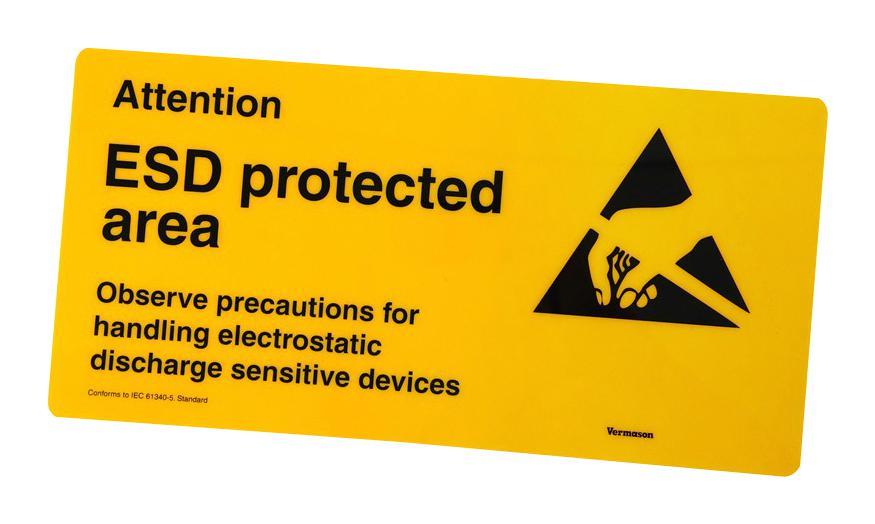
Introduction to ESD Trays ESD stands for “electrostatic discharge”.Ultrathin Wafer Pre-Assembly and Assembly Process Technologies: A Review Michael Raj Marks,1,2,* Zainuriah Hassan,2 and Kuan Yew Cheong3 1Infineon Technologies (Kulim) Sdn.Additional Information 6 of 19 Revision 2.com 1 AN-1060 International Rectifier • 233 Kansas Street, El Segundo, CA 90245 ! USA BARE DIE: HANDLING AND STORAGE By Richard Clark Introduction International Rectifier supply a range of power100V RDS(on) = 0.
A Complete Guide to ESD Protection
April 2015 DocID026684 Rev 2 1/7 www. An discharge as small as 30V can .When I was growing up, I often heard the phrase “stop giving me static,” uttered in angst by my mom.0) Seiko Epson Corporation 6 1.) @ IC = 50 A • 10 μs of short-circuit withstand time • Minimized tail current • Tight parameter distribution • Positive VCE(sat) temperature coefficient ApplicationsPCB Design and Assembly for Flip-Chip and Die Size CSP Vern Solberg STC-Madison Madison, Wisconsin USA Abstract As new generations of electronic products emerge they often surpass the capability of existing packaging andVixar Application Note VCSEL Die Handling and Packaging Page 4 of 11 3 Die Production and Delivery Vixar VCSELs in production are 100% tested before delivery to ensure performance matches
Standards & Documents Search
Title Document # Date; Requirements for Handling Electrostatic-Discharge-Sensitive (ESDS) Devices: JESD625C. For circuits that use semiconductor products, design the circuit so that it operates within the recommended operating conditions.
Box 3002 Los Alamitos, CA 90720.5D/3D technologies require designers to reduce electrostatic discharge (ESD) protection of the internal I/O interfaces. 10/2007 Additional Testing and Screening
Handling Bare Die
CSN-24: ESD Precautions for Die/Wafer Handling and Assembly Introduction Customer Service Note Electrostatic Discharge (ESD) Precautions for the Handling and . : AN00011329 – 25 Nov 21 1/14 Subject to change without notice United Monolithic Semiconductors S.4 Product selection., Kulim Hi-Tech .When you service this computer, always wear an electrostatic discharge (ESD) wrist strap that is properly connected to the rack frame or enclosure sheet metal. of Semiconductor Devices.
- New Player Here. Most Fun Faction To Play As?
- Dreirad Draisin Ebay Kleinanzeigen Ist Jetzt Kleinanzeigen
- Chapter 2 Multivariate Normal Distribution
- Envivas Als Bester Krankenversicherer Ausgezeichnet
- How To Cut Metal Using Angle Grinder Like A Pro
- Audi Bewerbung Prüfungsfragen | ᐅ Einstellungstest Audi: Das erwartet dich im Eignungstest
- Songtext Von Jimmy Dean , Jimmy Dean Lyrics, Songs, and Albums
- Custom Brochure, Pamphlet _ Best brochure design software
- Home Deluxe Infrarotkabine Redsun L Online Kaufen Bei Netto
- Hausarzt , Hausarzt Bonn-Beuel