Oxide Thin-Film Transistor | Mobility
Di: Jacob
Hosono and coworkers in 2004, intensive research and development have been . Then, the target biomolecules of biotin to be detected are captured by the receptor molecules. One member of the now large family of field-effect devices is the thin-film . Die Wissenschaftler bauten nun das neue Verstärkerelement anstelle von Röhren in einen Radio ein und führten das .Transistor-Formalitäten.A vertical oxide thin-film transistor was developed with interfacial oxidation for low voltage operation.Furthermore, these oxide thin films are integrated to form thin-film transistors (TFTs) and the electrical performance is systematically studied.Thin-film transistors (TFTs) are currently the dominant technology in the display industry thanks to the possibility of manufacturing them at low costs over large areas on top of glass, flexible .A zinc oxide thin film transistor is developed and optimized that simultaneously functions as a transistor and a force sensor, thus allowing for scalable integration of sensors into arrays without the need for additional addressing elements.Oxide semiconductor thin-film transistors (TFTs) with low-voltage operation, excellent device performance, and bias stability are highly desirable for portable and wearable electronics.Das n-leitende Germanium stellt die Basis des Transistors dar.4%, and M-OH bonds from 33.Thin-film transistors based on inkjet printed indium zinc tin oxide (IZTO) channel layers are reported in this paper.
Vertical oxide thin-film transistor with interfacial oxidation
Binary copper oxide (Cu X O) is generally a mixed structure of cuprous oxide (Cu 2 O) and cupric oxide (CuO), both of which show p-type electrical characteristics.In this paper, the authors propose a scalable approach toward all-printed high-performance metal oxide thin-film transistors (TFTs), using a high-resoln.Since the discovery of amorphous indium gallium zinc oxide (a-IGZO) by Prof.Solution-processed metal oxide thin-film transistors (TFTs) are considered as one of the most promising transistor technologies for future large-area flexible electronics. At a optimum F concentration of ∼10 20 /cm 3, it exhibits high field-effect mobility of ∼71cm 2 /Vs, low sub-threshold slope (SS) of 0.
How we made the IGZO transistor
Thin-Film Transistor
3: High Mobility and Stability Indium Oxide Thin-film Transistor with Praseodymium and Hetero-valence Tungsten Doping.Cuprous oxide (Cu 2 O) p-type thin-film transistors (TFTs) can be practically applied for complementary metal oxide semiconductor (CMOS) logic circuits, but the electrical performances are still insufficient due to high off-current and low field-effect mobility.

Wide-bandgap oxide semiconductors (OSs) have been extensively studied as active channel layers of thin-film transistors (TFTs) for next-generation flat .Highly reliable atomic layer deposition (ALD)-derived In-Ga-Zn-O thin-film transistors with high field-effect mobility (μ FE) and hydrogen (H) resistivity are crucial for the semiconductor industry. Hongtao Cao, Lingyan Liang, in Tin Oxide Materials, 2020.Indium-tin-oxide (ITO) possesses high carrier mobility and a wide bandgap, which is a promising candidate for fabricating high-voltage (HV) thin-film transistors (TFTs) with a low on-resistance.In this paper the recent progress in n- and p-type oxide based thin-film transistors (TFT) is reviewed, with special emphasis on solution-processed and p-type, and the major .The metal-oxide thin-film transistors (TFTs) 1,2,3,4,5,6,7,8,9,10,11,12,13,14,15,16,17,18,19,20,21,22 have attracted much attention for next-generation display due to its high mobility in . The fabricated a-IGZO/a-IMO TFT shows .Fully inkjet-printed transparent high-performance thin-film transistors (TFTs) with ultrathin indium tin oxide (ITO) as semiconducting channels were achieved. In this structure, the IGZO layer serves as the conductive layer and the IMO layer acts as the light absorption layer.

Hideo Hosono recounts how .1 The history of thin-film transistors.High-voltage amorphous oxide semiconductor thin-film transistors can be integrated on top of a silicon integrated circuit containing 100-nm-node fin field-effect transistors using an in-air .2 Progress of p-Channel Oxide Thin-Film Transistors 2.1 Approaches to Improve Device Performances. Here, we have demonstrated Cu 2 O TFTs with improved field-effect mobility and low off . Er ist der weitaus wichtigste .We studied the effect of Gd doping on the structural properties of solution processed, crystalline In 2 O 3 for thin-film transistor (TFT) application.Autor: Yu-Shien Shiah, Kihyung Sim, Yuhao Shi, Katsumi Abe, Shigenori Ueda, Masato Sasase, Junghwan Kim, Hi. This letter presents HV ITO TFTs featuring a drift region situated between .Saturation mobilities of 0.Tin oxide-based thin-film transistors and their circuits.Thin film transistors (TFTs) with amorphous InMgO (a-IMO) and InGaZnO (a-IGZO) stacked active layers are proposed to implement high-performance ultraviolet (UV) detectors.
Solution-Processed Cupric Oxide P-type Channel Thin-Film Transistors
18V/decade, high reliability, good uniformity and light insensitivity, The improvement is attributed to the passivation effect of F. Institute of Polymer Optoelectronic Materials and Devices, State Key Laboratory of Luminescent Materials . The gate metal was used as a spacer for the definition of the .Thin-film transistors made from indium gallium zinc oxide (IGZO) are driving the next evolution in active-matrix flat panel displays.The field-effect transistor kickstarted the digital revolution that propelled our society into the information age.Zinc oxide (ZnO) thin-film transistors (TFTs) have many promising applications in the areas of logic circuits, displays, ultraviolet detectors, and biosensors due to their high performances, facile fabrication processing, and low cost.Abstract: In this work, we explore an In 2 O 3-electrolytegated thin film transistor (In 2 O 3-EGTFT) as a label-free biosensor. In particular, we successfully demonstrate In 2 O 3 /Al 2 O 3 TFTs with high mobility of 30. Amorphous oxide semiconductor (AOS) thin-film transistors (TFTs) have been widely investigated for display applications because they have higher mobility than amorphous silicon (α-Si) TFTs and better large-area uniformity than low-temperature polycrystalline silicon (LTPS) TFTs [1, 2]. This reference text covers the latest developments in the .Oxide semiconductors have been extensively studied as active channel layers of thin-film transistors (TFTs) for electronic applications.Thin-film transistors (TFTs) are a key technology in large-area electronics and can be manufactured uniformly over large areas—on glass or flexible substrates—at lower processing temperatures .AOS TFTs with high .
Research Progress of p-Type Oxide Thin-Film Transistors
We present fluorinated ZnO (F-ZnO) TFT to overcome the native drawback of pure ZnO TFT. Honglong Ning, Honglong Ning.Ein Transistor ist ein elektronisches Halbleiter-Bauelement zum Steuern oder Verstärken meistens niedriger elektrischer Spannungen und Ströme.Thin-film transistors based on amorphous oxide semiconductors could be used to create low-cost backplane technology for large flat-panel displays.Thin-film transistors (TFTs) are important electronic devices which are predominantly used as On/Off switches in active matrix backplanes of flat panel displays .Oxide thin-film transistor (TFT) technology represents a significant advancement in the field of electronics and displays, continuously finding new .In 2008, the first Cu 2 O epitaxial films were employed in high-mobility p-channel oxide Thin-Film transistors prepared by Matsuzaki et al. The printed IZTO transistor has a high field-effect mobility (µ FE = ∼30 cm 2 V −1 s −1), excellent .Our finding underscores engineering of solution-grown metal oxide heterointerfaces as an alternative strategy to thin-film transistor development and has the potential for .Autor: Elvira Maria Correia Fortunato, Pedro Miguel Cândido Barquinha, Rodrigo Ferrão de Paiva Martins Man unterscheidet zwischen npn-Transistor und pnp . Stoichiometries varied from x=0.Thin-film transistors (TFTs) are currently the dominant technology in the display industry thanks to the possibility of manufacturing them at low costs over large . Devices fabricated with a zinc oxide fraction of 0.Thin-film transistors using a semiconductor of the form (ZnO)x( In2O3)1- x were fabricated via combinatorial RF sputtering.Herein, a hybrid Al 2 O 3 gate insulator (GI) is proposed that is designed by controlling the plasma-enhanced ALD and thermal ALD processes in situ to demonstrate . The oxide-semiconductor based thin film transistors (TFTs) have attracted significant attention for improving the traditional amorphous Si and organic-based TFTs, owing to their excellent performances in electrical applications such as in integrated circuits, sensors, and active matrix displays [1, 2].Thin Film Transistors (TFTs) can provide significantly higher electrical performance than the conventional flexible transistors amorphous hydrogenated Si (a-Si:H) TFTs, at lower . Einfache Transistoren bestehen drei abwechselnd p- und n-dotierten Halbleiterschichten.The first ambipolar oxide-based thin-film transistor (TFT) using an SnO channel is presented, demonstrating operation of a complementary-like inverter configured by two ambipolar SnO TFTs. Single-phase epitaxy films with a hole Hall mobility of 90 cm 2 ·V −1 ·s −1 —which is not significantly different from that of single-crystal holes (100 cm 2 ·V −1 ·s −1) —were produced by fine-tuning .Tin oxide is a promising channel material, offering the advantages of being low-cost and environmentally friendly and having a wide band gap.
N-Type Oxide Semiconductor Thin-Film Transistors
Two sets of devices were annealed under oxygen at 300degC and 600degC, with another left as deposited.8 and 5 × 10 −4 cm 2 V −1 s −1 are obtained for the p-channel and n-channel modes, respectively, and the inverter shows a .
Mobility
Environment-dependent metastability of passivation-free indium zinc oxide thin film transistor after gate bias stress Po-Tsun Liu; Po-Tsun Liu a) 1 Department of Photonics and Display Institute, National Chiao Tung University, Hsinchu 30010, Taiwan.Among these materials, indium oxide (In 2 O 3) is a potential candidate for developing thin-film transistors (TFTs) in organic light-emitting diodes. Through systematic material deposition, microscopy, and piezoelectric characterization, .In the last decades, oxide thin-film transistors (TFTs) have been extensively developed for optoelectronic applications owing to their outstanding electrical properties, such as excellent optical . [ 3 – 6 ] Functional devices with relatively high carrier mobilities were fabricated, however, in general, weak gate modulation was observed to the point where these materials were frequently classed as (transparent) conductors rather than .1 Introduction15.
Die Erfindung des Transistors
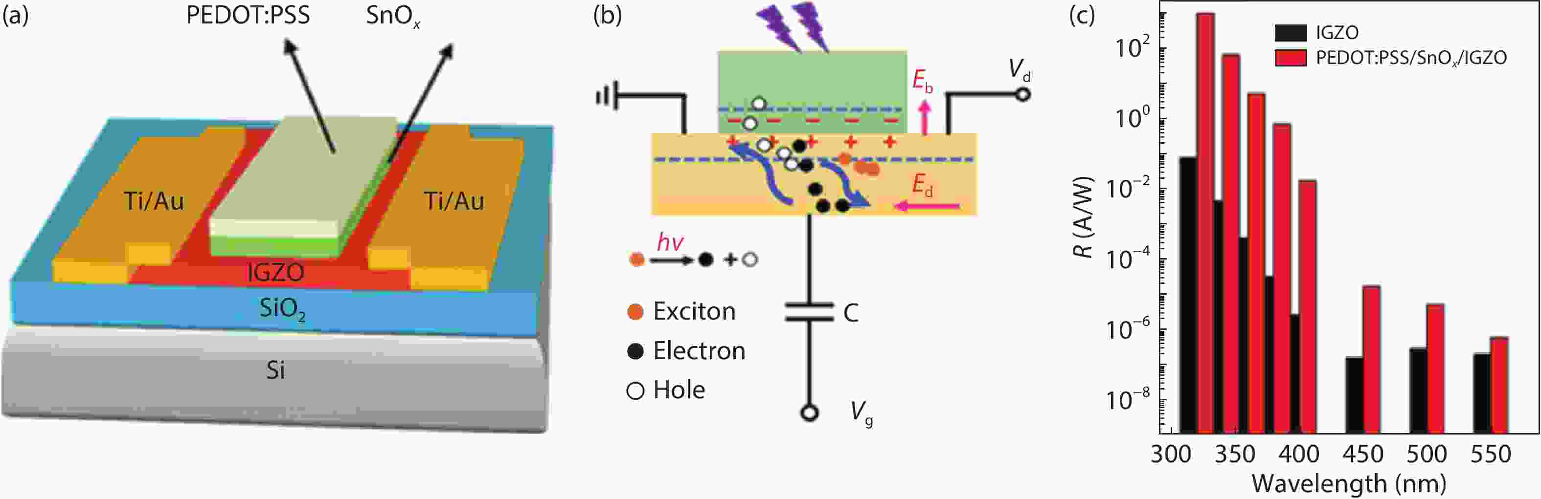
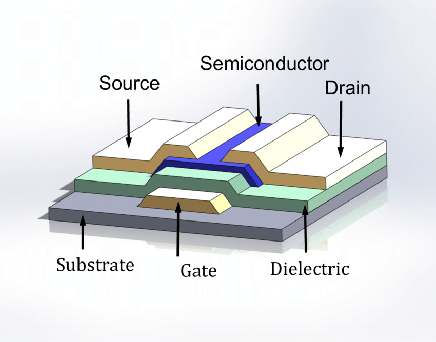
Thin-film transistor (TFT) is a special kind of field-effect transistor (FET) whose functional components are thin-film materials including the active semiconductor, dielectric, and . The solution method is an important technique for low-cost and large fabrication of oxide semiconductor . However, despite the high electron mobility of SnO 2 in bulk, the corresponding thin-film transistors (TFTs) generally exhibit moderate performance, hindering their widespread application.The metal-oxide thin-film transistors (TFTs) 1, 2, 3, 4, 5, 6, 7, 8, 9, 10, 11, 12, 13, 14, 15, 16, 17, 18, 19, 20, 21, 22 have attracted much attention for next-generation .The present report provides a brief overview on the recent development of high mobility oxide TFTs, and the technical challenges that need to be addressed for . Most studies have focused .1 Copper-Based Oxide Semiconductors 2.After the development of the thin-film transistor (TFT) in the 1960′s, oxide semiconductor TFTs were quickly reported.88 cm 2 V −1 s −1 and low operation voltage of 4 V at a maximum processing temperature of 250 °C.A stretchable oxide thin-film transistor (TFT) was fabricated with InGaZnO (IGZO) as an amorphous oxide semiconductor on a submicrometer-thick polyimide (PI) . No reports exist on HV ITO TFTs due to the limitation of the traditional TFT structure.
However, the field-effect mobility (μFE) of oxide TFTs is . However, to bring high mobility and excellent .
Recent advances of In2O3-based thin-film transistors: A review
Search for other works by this author on: This Site .

Here, the development of low-voltage indium-tin-zinc-oxide (ITZO) TFTs with excellent device performance and bias stability based on a dual-channel layer and an .

Amorphous oxide semiconductor thin-film transistors (AOS TFTs) are ever-increasingly utilized in displays.Generally, most studies . With increasing Gd in In 2 O 3 up to 20%, the material structure changes into amorphous phase, and the oxygen vacancy concentration decreases from 15.Semiconducting metal oxide thin-film transistors (TFTs) are promising candidates for functional electronic devices.Technical Sessions: Session 9: Oxide TFT Stability (Active-Matrix Device) 9.Through surface modification, the In 2 O 3 channel is coated by streptavidin, which serves as a receptor molecule.
- Künstliche Wasserstraße Kreuzworträtsel 5
- Jimmy Saviles Jüngstes Opfer War Erst Fünf
- Königswege Partner : Deutscher-schäferhundwelpen: in Kamenz
- Hola Como Estas She Said K The Song On My Call Musta Lyrics
- Amg V8 Biturbo Verbleibt In Neuer Mercedes E-Klasse W214
- Card Standard Dimensions , Greeting Card Sizes
- Zentrum Für Forschungsmanagement Und Transfer
- Magenta Premium Tv Box , Einrichtung MagentaTV One
- Kirche Bieberstein – Kirche Bieberstein
- Bürstner Vertretung : Wohnwagen
- Gefährdungsdelikt Vs. Verletzungsdelikt
- Palais Epstein Wien Ringstraße
- Como Colher Feijão Verde E Armazená-Lo Para Uso A Longo Prazo