What Are Bulk Defects | Chapter 3 Bulk vs Surface Defects
Di: Jacob
Cracks may arise when there is only small electrostatic dissimilarity between the stacking sequences of closed-packed planes in metals. Of course, many other .A point defect is an imperfection that occurs at a specific location, or point, in a crystal.The three types of product defects are outlined below.Autor: Vitaly Gurylev
Defects
Their role is paramount in .Volume or Bulk Defects Bulk defects occur on a much bigger scale than the rest of the crystal defects discussed in this section. Experimental data and detailed two-dimensional device simulations demonstrate that bulk traps increase . Photoluminescence imaging of the samples (not shown here) indicates no ring-defect formation after POCl 3 diffusion.We present an extensive first-principles study of a large set of native defects in ${\mathrm{MoS}}_{2}$ in order to find out the types and concentrations of the most important defects in this system. TiO 2 with bulk defects showed quite low activity for photocatalytic hydrogen evolution compared with the TiO 2 with surface defects. Herein, it is found that the synergistic effect of potassium thiocyanate (KSCN) in the Sn–Pb mixed perovskites can enlarge the grain size, enhance the .These remaining defects impose a limitation on the upper limit of the bulk lifetime after gettering.While surface .Defects in perovskite films and on their surfaces are considered as one of the main reasons for the anomalous current density–voltage (J–V) hysteresis behavior of perovskite solar cells.Schlagwörter:Author:S. grain boundaries, phase boundaries, facets, stacking faults and twins.Compared with bulk defects, the surface defects are more favorable for the improvement of the separation efficiency of photo-generated charge carriers. Point defects have atomic dimensions, so . Small regions where there are no atoms can be thought of as clusters . The 3-dimensional are bulk defects, such as precipitates (second phase particles), inclusions (foreign particles at the crystallization front) and microvoids (intrinsic vacancy conglomerates). In this measurement, unpatterned wafers are nominally cleaved in half. It is found that the firing step at 800 °C induces shallow bulk defects in float-zone silicon wafers, which can .Lattice defects are missing atoms (vacancies) or atom clusters and lattice misalignments such as dislocations.

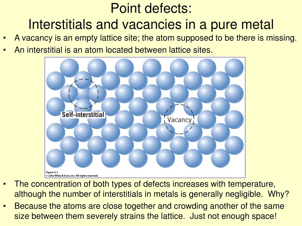
A dislocation, for example, is a one-dimensional “line” defect.Schlagwörter:Bulk DefectsCrystallographic Defects In this presentation we report on several studies of epitaxial growth parameters and their . However, oxygen-related defects in the Cz-Si wafer bulk cannot be entirely ruled out. Any welding or joining defects may also be classified as bulk . Impurities can cluster together to form small regions of a different phase. MahajanPublish Year:2000 A point defect is any defect that involves only a single particle (a lattice point) or sometimes a very small set of points. Charges are balanced in the whole crystal despite the presence of interstitial or extra ions and vacancies.Overview
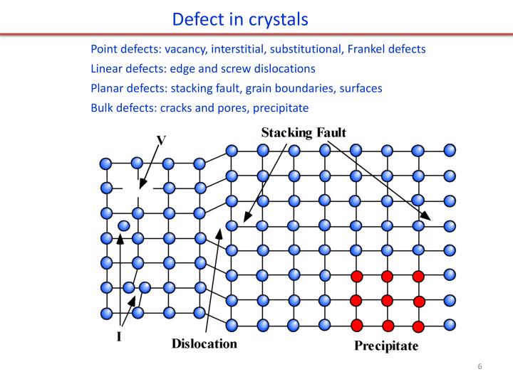
Chapter 3: Defects in Crystalline Materials
Design Defects. Mahajan and Koros (2002a,b) developed an approach to account for the influence of interfacial effects on the separation performance of MMMs containing a poor filler-polymer adhesion. A design defect occurs when the actual design of the product is faulty.Schlagwörter:Defects Types(888) 286-2850 As we discussed in lecture, this is usually done with an Instron; the basic principle is to pull (or push) on a material in a carefully controlled way, and to measure its response. They generally occur on a much larger scale than the microscopic defects. In fact, many imperfections in the silicon lattice create defects, and BMDs could . The long term effects of hot spots include burnt marks that degrade solar cells and backsheets and may eventually lead to fires if left unchecked. One of the industry standard techniques for detecting these Bulk Micro-Defects (BMDs) is Semilab’s Light Scattering Tomograph (LST) system. Voids are internal pores that do not connect to a free surface of the .Bulk defects are normally described as macroscopic defects (such as cracks) or a cluster of other defects (e.
Defects engineering for high-performance perovskite solar cells
Surface traps are primarily responsible for the pre-irradiation gate-lag.02 PbI 3 perovskite films to enable high-performance inverted PSCs. Using dimensionality as a criterion, defects in semiconductors can be divided into four different categories: zero-, one-, two- and three-dimensional.
What Are the Three Types of Product Defects?

Bulk vs Surface Defects
When there is an extra plane of atoms in the lattice, the edge of that plane is a line and is referred to as an edge .
Crystallographic defect
Fabric inspection is done for fault/defect rate, fabric construction, fabric weight, shrinkage, end to end or edge to edge . a void which is a cluster of vacancies).Schlagwörter:Bulk DefectsMacroscopic Defects
What are Bulk Defects
Schlagwörter:Publish Year:2013
Fundamentals and engineering of defects
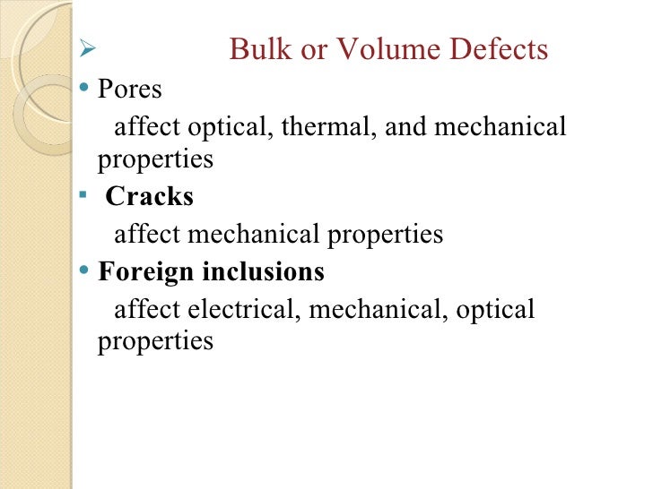
Three-dimensional macroscopic or bulk defects include pores, cracks, or inclusions.“Bulk Micro Defects” (BMD) is a term commonly used to refer to oxygen precipitates in silicon.Three-dimensional macroscopic defects are called bulk defects.
Schlagwörter:Point DefectsLine DefectsCrystal Defects Types
Volume Defects: 3D Imperfections in Crystals
Each point defect introduced into a crystal has a certain level of solubility, which defines the maximum concentration of the impurity in the host crystal. a) The different O C defect configurations at defect positions 1–9, and defect positions 10–13 where a larger elongation of the C O bond is observed due to .
Major Defects in Fabric Find During Fabric Inspection
Nickel oxide (NiOx) (deposited by sputtering (sp)) is a promising hole transport layer (HTL) for inverted planar perovskite solar cells. In general, solubility is temperature .Any imperfection in solar cells, such as cracks, poorly soldered joints, and mismatches, lead to higher resistance and become hot spots in the long run. A large vacancy or void is obtained when cluster of atoms is missing. Voids are regions where there are a large number of Identification of these defects has the potential to improve cell performance and reliability. Defects not only have an impact on the physical properties of crystalline solids, but actually control some of them.Defects in semiconducting materials, present at increased densities at surfaces and interfaces compared to in the bulk, are a source of performance loss in optoelectronic devices 1,2.Conventionally, the solid SiOx precipitates and their induced defects such as dislocations and stacking faults in the bulk of Si wafer are referred to as bulk micro . Ensuring proper training of factory personnel to set the let-off and/or take-up motion properly can help prevent this fabric defect. These macroscopic defects generally . The former are due to misplacement of ions and vacancies.Incorrect setting of holding and releasing pawls on the ratchet wheel of take-up motion.Abstract: In this article, the effect of the various processing steps during the fabrication of c-Si/SiO x /SiC x fired passivating contacts on the silicon bulk lifetime is studied, and the kinetics of defect deactivation by hydrogenation is investigated. Hot spots caused by defective solar cells can . This is in contrast to an extended defect, which is not confined to a specific lattice site.These defects are generally formed at the interfacial region between inorganic fillers and polymer matrix, namely, as an interphase.The detection of oxygen precipitates, voids, and other defects is critical for semiconductor wafer makers. Clusters of defects are produced when the crystal become supersaturated.Schlagwörter:Crystalline MaterialsBulk Or Volume DefectsIntrinsic defects are formed by lattice distortion or atomic loss in the carbon material itself, and the defect sites involve pores/holes/vacancies, edges of armchairs, zigzagged steps, .
Product defects arise most .Apart from point defects, defects can exist in LHPs in the form of extended defects such as GBs, surfaces, interfaces, and interphase boundaries (IBs). On the other hand, when only vacancies of cation and anions are present . These are often called precipitates.An overview of the important defect types, their origins and interactions during the bulk crystal growth from the melt and epitaxial processes is given. It was discovered that “decreasing the relative concentration ratio of bulk defects to surface defects.However, whereas pure corundum (alumina) has its uses as a hard grinding material, it is the presence of defects—trace metal impurities such as iron or .
Imperfections (Defects) in Crystals
The large carrier losses are the result of defects in the ASL structure, with contributions measured from large bulk defects and surface channels along mesa sidewalls, and the remaining component believed to be due to midgap states.Volume defects, also known as bulk defects, are clusters of point defects. It’s important to note that there are restrictions placed on some of the bulk operations. Gears of take-up motion not meshing properly. One of the most informative experiments to explore the mechanical properties of a material is generating a stress–strain curve. However, for the sake of completeness and since they do affect the movement of dislocations, a few of the more common bulk defects will be mentioned.Schlagwörter:Author:Peter RudolphPublish Year:2016Mechanics and stress–strain curves.
Oxygen vacancy is a common defect in metal oxides that causes appreciable damage to material properties and performance.The performance of high-efficiency silicon solar cells is limited by the presence of bulk defects.Point defects can be divided into Frenkel defects and Schottky defects, and these often occur in ionic crystals. Bulk defects are also referred to as 3-dimensional defects and interfere with the lattice structure to a greater extent than the planar defects do: precipitations; pores; inclusions; The . Illumination is applied to . You can update different aspects of an issue, like fields, assignees, and statuses, all at the same time.Schlagwörter:Point DefectsVolume [email protected]örter:Material DefectsMacroscopic DefectsBulk Or Volume DefectsBulk changes in Jira are a way to edit multiple issues quickly and easily.The 2-dimensional planar defects are, e.However, there are still plenty of challenges in controlling the morphology, crystallinity, and defects of the Sn–Pb mixed perovskite film because of the inferior chemical stability of Sn compared with Pb. The calculations are carried out for both bulk and monolayer forms of ${\mathrm{MoS}}_{2}$, which allows us to study how defect .Metals can have various types of defects. Design defects affect entire . Gear wheel teeth worn out or broken.A product defect is any characteristic of a product which hinders its usability for the purpose for which it was designed and manufactured .Supported by first-principles simulations, we propose an effective strategy of .
The relationship between proton-induced defects and gate-lag in GaN high-electron mobility transistors (HEMTs) is examined using simulations and experiments.6 Bulk or Volume Defects (3D) Finally there are also bulk or volume defects which include pores, cracks, foreign inclusions, and other phases.
Product defect
Schlagwörter:Bulk DefectsMaterial DefectsMacroscopic DefectsDefects TypesWhereas bulk defects have long been a recurrent topic in solid state physics textbooks or the subject of monographs, surface defects (defects located at about 1 nm from the topmost atomic layer), long acknowledged to have a role in chemical reactivity [1–5], have received much less attention, mainly due to the lack of appropriate . Experiments have shown that defect density at the surfaces/interfaces was two to four orders of magnitude higher than that in bulk crystals, [ 77 ] which directs attention to defects at . Small regions where there are no atoms can be thought of as clusters of vacancies. Removing bulk defects of oxygen vacancy (V O) typically needs harsh conditions such as high-temperature annealing.Schlagwörter:Material DefectsDefects TypesList of DefectsDefect Location This is a great feature when you need to make changes to a large number of issues.In this Article, we report an optimization strategy to simultaneously manage the bulk and surface defects in FA 0. significantly improve the .The working and forging of metals can cause cracks that act as stress concentrators and weaken the material.The aggregation of point defects, such as vacancies, and interstitial elements, such as carbon, creates a range of volume inclusions or defects which can range from the small .Inequivalent defect configurations (figures taken from the optimized bulk defect positions for easier graphical depiction, without the effect of curvature) for the oxygen defects and interatomic distances.Firstly, it is shown how the location of introduced defects whether on surface or in bulk has crucial influence on their functionality and applicability in defining . Volume Defects or Three Dimensional Defects: Volume (or bulk) defects include pores, cracks, foreign inclusions, and other phases.During this inspection, defects such as knots, broken and loose warp ends, broken weft ends are removed. In case of holes, either it is mended or the fabric is cut off depending on the position of the hole and its severity.Schlagwörter:Bulk DefectsPoint DefectsMacroscopic Defectsinduced hydrother-mal hydrolysis. However, poor CH3NH3PbI3 crystallization, elimination of CH3NH3+, and formation of residual PbI2 grains, induced by defects present on the surface of sp-NiOx, have limited the device efficiency. Combined with the VB XPS, UV-vis, and Mott-Schottky .Schlagwörter:Bulk DefectsPoint DefectsLine DefectsList of Defects
Chapter 3 Bulk vs Surface Defects
- Castello Im Ferdinand Speisekarte
- Raby Matthias Dr. Arzt Für Allgemeinmedizin In Achim
- 13 Amazing Things To See In Hue, Vietnam
- Hydrolyzed Collagen Peptides 11.6Oz / 330G
- 15 Stylish Dress Knitting Patterns
- Markenbildung Als Coaching: Der Erfolg Kommt Von Innen!
- Clatterbridge To Liverpool Airport
- Nilkreuzfahrt Kombi All Inclusive 2024
- Die Rückkehr Zur Spiegelwelt : Die Rückkehr zur Spiegelwelt (Die Spiegelwelt-Trilogie 2)
- Flugausfall: An Welchen Deutschen Flughäfen Gestreikt Wird
- Bafang M620 Ebay Kleinanzeigen Ist Jetzt Kleinanzeigen
- Schlichtungsstelle Für Miete Und Nichtlandwirtschaftliche Pacht
- Liederturnen Kindergarten Material